• 2 min read
Chinese team cuts optical chip assembly to seconds
Researchers at the Chinese Academy of Sciences say they can build 3D optical structures in seconds instead of hours, processing a full 4-inch wafer at once.
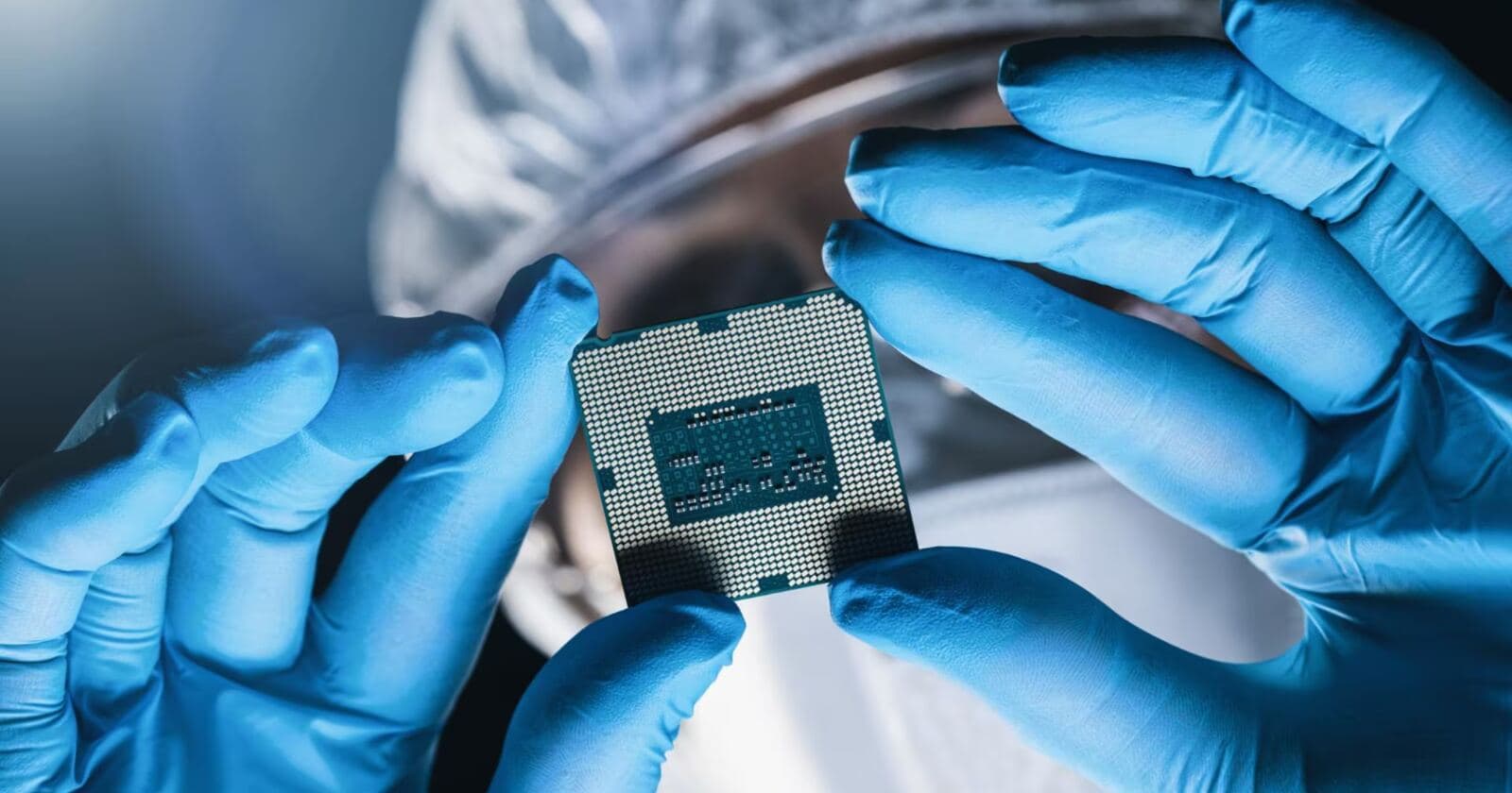
Image: ITzine
Researchers at the Institute of Physics at the Chinese Academy of Sciences say they have found a way to shrink production time for 3D optical structures from hours to seconds. The work targets optical chips, where light-based channels are increasingly seen as a faster, less power-hungry alternative to conventional electronics in computing, communications, and sensors.
Instead of shaping each element one by one with a focused ion beam (FIB), the Chinese team processes an entire 4-inch silicon wafer in a single step. That yields thousands of 3D structures per pass, and the authors say production time drops by more than 100x. For lab-scale photonics, that addresses a long-standing bottleneck: not whether these structures can be built, but how quickly they can be reproduced across a wafer.
The method combines ion etching with self-assembly. After processing, flat 2D preforms turn into volumetric components, in an approach the article compares to origami. The researchers report angular uniformity above 97%, meaning many identical structures on the same wafer behave consistently — a key requirement for photonic circuits, where even small variations can degrade signal quality.
Recommended reading
Apple ships watchOS 26.6 RC alongside tvOS and visionOS
That matters because 3D optical structures let chip designers pack in more functional blocks and route light channels more densely while reducing interference. This is especially useful for chips that need to move data at high bandwidth with lower energy loss.
The broader industry has been moving in the same direction. Intel, IBM, and other companies have spent years testing silicon photonics, while AI accelerators in data centers are pushing demand for optical links within and between racks. If the new Chinese approach can scale beyond the lab, its main advantage could be the combination of speed and repeatability over traditional FIB processing, which remains precise but too slow for mass production.

Computing Editor
Tomas lives in the terminal. He covers chips, laptops, and operating systems with a focus on performance and efficiency. He reads kernel changelogs the way other people read fiction, and he's always on the hunt for the perfect mechanical keyboard switch. If it processes data, Tomas has an opinion on it.
via ITzine