• 2 min read
Russia Tests Maskless 150 nm Chip Lithography Tool
Russia has built a maskless electron-beam lithography system for 150 nm chips. Two prototype units are now in testing for about four months.
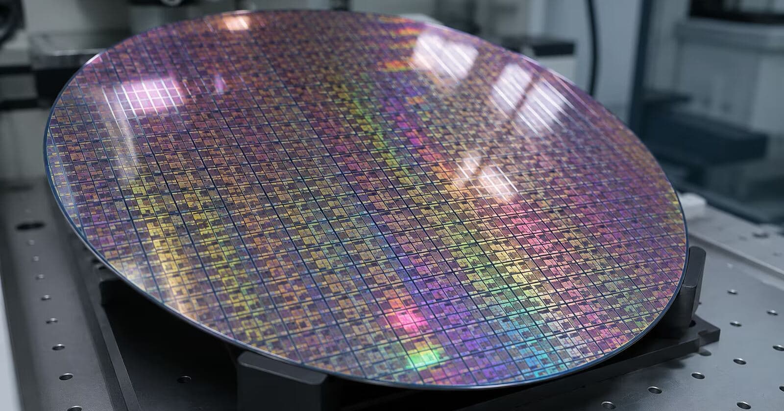
Image: ITzine
Russia has built an electron-beam lithography system with 150 nm design rules, aimed at chip prototyping, research, and small production runs rather than high-volume processors from TSMC or Intel. The developer is the Zelenograd Nanotechnology Center, and two prototype units are now undergoing integrated testing that is expected to last about four months.
The main feature is straightforward: the system works without masks. That means circuit patterns can be written directly onto silicon and other substrates, and photomasks can also be made without a separate mask cycle. Electron-beam lithography is slower than photolithography, but it avoids the need to manufacture a separate mask for every design. For R&D and specialized electronics, that tradeoff can be more useful than raw speed.
For advanced microelectronics, 150 nm is no longer cutting-edge. But for lab work, process development, and limited chip batches, it remains practical. The maskless approach also shortens the path from design to test production, especially for customers that need dozens or hundreds of chips with specific parameters rather than thousands of identical dies.
Key details from the project:
- Design rules: 150 nm
- Technology type: electron-beam lithography
- Operating mode: maskless
- Status: two prototype units in testing
- Testing period: about four months
Zelenograd Nanotechnology Center chip equipment plans
This is not the center’s first move to fill gaps in the manufacturing chain. It previously presented a domestic 350 nm photolithography machine, and it is also developing equipment for 130 nm processes. The strategy appears to be a lineup of tools for different tasks rather than a single universal system.
Recommended reading
Russia unveils AA battery with wireless Qi charging
By global standards, 150 nm looks dated, with major chipmakers long since moving to far finer nodes. But the source argues that equipment in this class still matters in Russia, where imported systems can face restrictions and universities, research institutes, and industrial users may value access to the process more than top-end specifications.
The broader backdrop is funding. Earlier reports said the developer of the first Soviet atomic bomb received nearly 1 billion rubles to build modern chipmaking equipment. If testing succeeds, the next step will be refining the machine and deploying it in applied projects, a key test of whether Russia can cover at least part of its prototyping and small-batch manufacturing needs without relying on imports.

Computing Editor
Tomas lives in the terminal. He covers chips, laptops, and operating systems with a focus on performance and efficiency. He reads kernel changelogs the way other people read fiction, and he's always on the hunt for the perfect mechanical keyboard switch. If it processes data, Tomas has an opinion on it.
via ITzine