• 2 min read
Silicon photonics clears a key hurdle with material stacking
Researchers say micro-transfer printing can add new materials to silicon photonics chips, opening a path to faster data links and more complex optical systems.
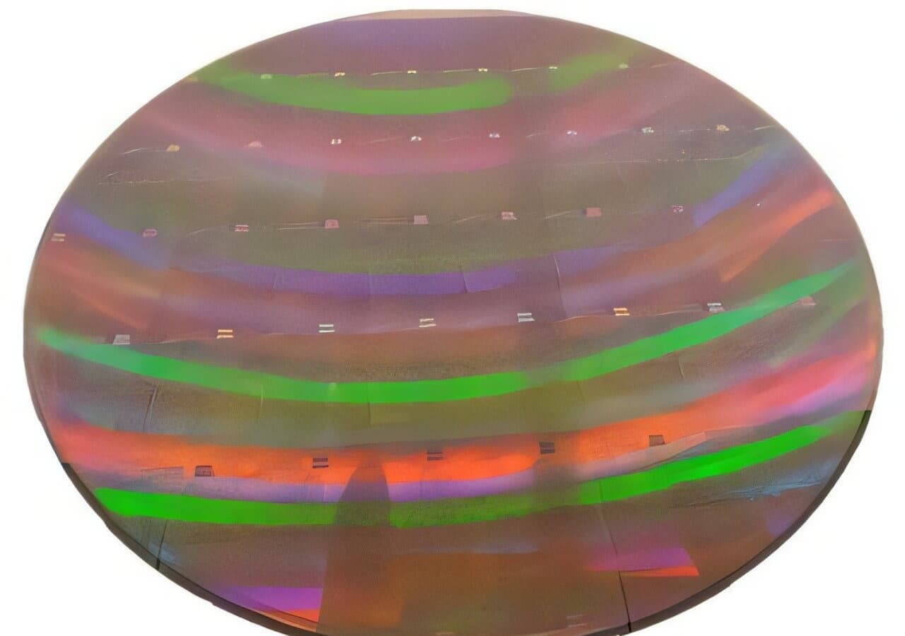
Image: iXBT
A major constraint in silicon photonics may be starting to fall away. Researchers report that micro-transfer printing (MTP) can combine silicon photonic chips with other semiconductor materials, a step that could help build faster data-transfer systems as bandwidth pressure grows inside computing hardware.
The work, published in the Journal of Lightwave Technology, targets a longstanding problem: standard CMOS manufacturing does not make it easy to integrate materials with very different optical properties onto silicon chips. That matters because silicon photonics, while already widely used in photonic integrated circuits (PICs) for telecommunications and data centers, cannot handle every function needed in advanced photonic systems. One example is on-chip light generation, which requires other materials such as III-V semiconductors and lithium niobate.
With MTP, thin-film devices are first fabricated on a separate source wafer. A specialized elastomer stamp then picks up selected components and places them onto a target silicon wafer. The parts are fixed in place through adhesive or direct bonding, creating a single photonic system made from multiple materials.
The core advantage is manufacturing flexibility: different parts of a photonic chip can be built independently using the best process for each material, then assembled into one architecture. According to the researchers, that could enable silicon photonic systems that integrate lasers, modulators, and other components that have been difficult to combine on one platform.
Recommended reading
Self-assembling thin-film electronics come from Japan
The paper points to several demonstrated uses of MTP already, including:
- systems for optical and microwave signal processing
- gallium arsenide (GaAs) lasers for virtual reality, quantum technologies, and microwave photonics
- integration of lithium niobate modulators with silicon nitride photonic circuits
The authors also described a pilot line aimed at adapting key MTP steps for industrial-scale manufacturing. The remaining challenges are stability and production maturity: improving component yield, reliability, manufacturing speed, and the broader production infrastructure needed for mass deployment.

Frontier Editor
Dan is our resident futurist, covering electric mobility, space exploration, and the smart home. He's interested in atoms just as much as bits. Whether it's a new battery chemistry, a reusable rocket, or a protocol that finally makes IoT devices talk to each other, Dan breaks down the engineering that pushes humanity forward.
via iXBT