• 3 min read
High-Bandwidth Flash targets AI weight storage
HBF applies HBM-style stacking to NAND flash, aiming for up to 1.6 TB/s reads for AI inference workloads where model weights are mostly read-only.
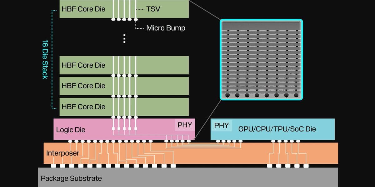
Image: Hacker News
Large language models are pushing memory demand so hard that chipmakers are expanding HBM and DRAM production, with one new fab scheduled to start production in 2027. But that pressure is also opening the door to alternatives, including High Bandwidth Flash (HBF) — a stacked version of NAND flash aimed at storing model weights more efficiently.
The idea is to borrow from High Bandwidth Memory: stack multiple dies to boost both capacity and throughput. In this case, the underlying media is the same kind of flash used in SD cards, thumb drives, smartphones, and SSDs.
“People ask, 'How in the world does this make a grain of sense? Flash is enormously slow,'”
Handy said NAND is especially weak on writes, but reads can be pushed much higher. As he put it, High Bandwidth Flash is designed to do exactly that.
Flash stores data as trapped electric charge in arrays of floating gate transistors, organized into blocks and pages rather than individually addressable bytes. It is non-volatile, so data remains without power. That makes it dense and efficient for long-term storage, but much slower to write than DRAM, which uses capacitors that can be refreshed quickly.

Recommended reading
Linus Torvalds' Nvidia broadside looks very different now
Today’s latest flash interface standard supports up to 4.8 GB/s per die. By comparison, DDR5 reaches up to 70.4 GB/s per DIMM, and HBM4E can hit 3.6 TB/s per stack — about a 750-fold bandwidth advantage over flash.
Sandisk and SK Hynix HBF plans
According to Hoshik Kim, senior vice president of memory systems research at SK Hynix, HBF uses advanced 3D packaging and vertical stacking to deliver far more bandwidth than standard NVMe storage. Sandisk has already published fact sheets for a first-generation HBF product, though shipping is still at least a year away.
Sandisk says its first stack will offer:
- up to 16 NAND flash chips
- up to 512 GB per stack
- up to 1.6 TB/s read bandwidth
Its roadmap projects 2 TB/s for a second generation and 3.2 TB/s for a third generation.
Why HBF is aimed at inference
HBF is still slower than the HBM used with high-performance GPUs, so its main use case is not AI training. Training constantly reads and writes across billions or trillions of weights, making flash a poor match.
AI inference is different. Once trained, model weights are effectively read-only, so flash’s weak write performance matters less. Kim said static multibillion-parameter weights and even precomputed KV cache data could sit in an HBF tier, freeing HBM to act as a high-speed scratchpad.
“If you set that up right, you can get an awful lot of good performance out of that—that’s just basic caching. It’s one technology that I’m expecting to go places.”
The technology is still early. On 25 February 2026, Sandisk and SK Hynix launched a joint effort to standardize HBF through a dedicated workstream in the Open Compute Project. A publication timeline for the standard has not been set. Kim said HBF should be seen as complementary to HBM, with the potential to ease HBM capacity bottlenecks, reduce the number of accelerators needed for large models, improve energy efficiency, and cut costs for inference infrastructure.

Enterprise Editor
Marcus follows the money. He covers enterprise software, cloud architecture, and the tectonic shifts in Big Tech strategy. He translates dense earnings calls and complex M&A activity into actionable insights about where the industry is actually heading. If a tech giant makes a silent pivot, Marcus is usually the first to notice.
via Hacker News