• 2 min read
Micro-transfer printing could unlock richer silicon photonics
A new study says micro-transfer printing could bring III-V semiconductors and lithium niobate into CMOS-compatible silicon photonics at scale.
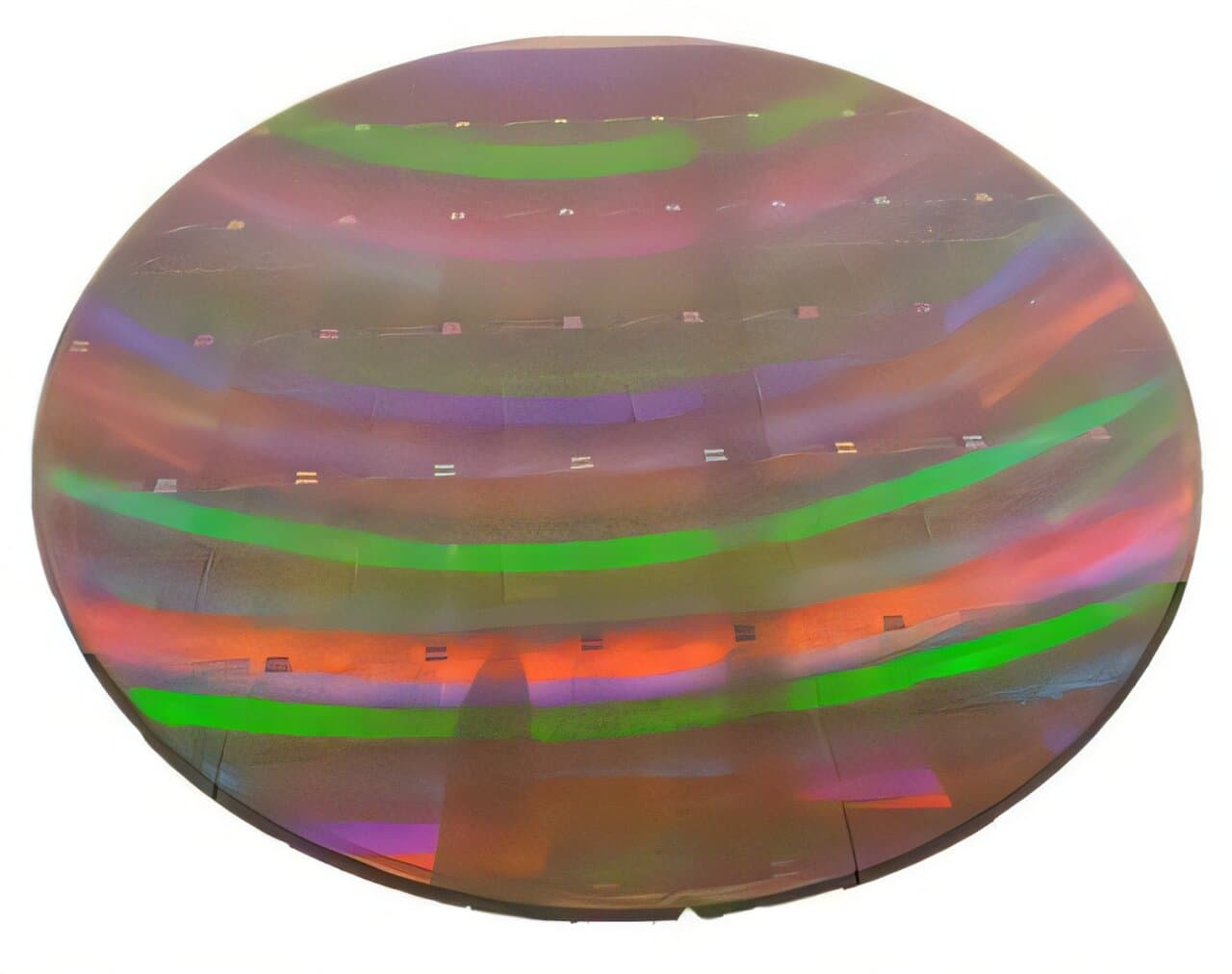
Image: TechXplore
Conventional electrical interconnects are becoming a major bottleneck as AI and the computing infrastructure around it demand more bandwidth. A new study in the Journal of Lightwave Technology points to micro-transfer printing (MTP) as a way to push silicon photonics further by combining silicon with materials that standard CMOS manufacturing cannot normally accommodate.
Silicon photonics is already widely used for photonic integrated circuits (PICs), especially in telecom and datacom, because it sends data with photons instead of electrons and fits existing semiconductor production lines. But that same CMOS compatibility is also a constraint: conventional group-IV semiconductor materials cannot cover every function needed in advanced photonic systems, particularly on-chip light generation.
That is where materials such as III-V semiconductors and lithium niobate (LiNbO₃) come in. According to Ir. Ye Chen of Ghent University—imec, Belgium, MTP is emerging as a flexible route to wafer-scale heterogeneous integration.
“Among the various approaches being pursued for enabling wafer-scale heterogeneous integration, MTP is an emerging, highly versatile technique that combines benefits of die-level assembly with wafer-scale processing.”
The process starts by making thin-film devices, or coupons, on a dense source wafer. A sacrificial release layer is selectively etched, an elastomeric stamp picks up multiple devices, and those devices are then printed onto a target wafer before being fixed in place through adhesive or direct bonding.
Recommended reading
Russia Tests Maskless 150 nm Chip Lithography Tool
The paper highlights several recent demonstrations, including:
- a fully integrated silicon photonic engine processing both optical and microwave signals using indium phosphide (InP) lasers
- gallium arsenide lasers integrated with silicon nitride waveguides for virtual reality, quantum technologies and microwave photonics
- widely tunable narrow-linewidth InP lasers integrated with Si3N4 waveguides for coherent communications and light detection and ranging
- wafer-level integration of LiNbO3-based modulators with Si3N4 photonic circuits
- heterogeneous electronic-photonic optical receiver platforms
The study also describes a new pilot line aimed at key MTP steps for large-volume manufacturing. The authors say major hurdles remain, including yield, reliability, throughput, and building a scalable manufacturing ecosystem.
“The MTP technology is still in its early stages of commercial application; however, we believe that consistent advancements will soon lead to large-scale industrial manufacturing, paving the way for advanced silicon photonics that will benefit several industries.”
The paper is titled “Micro-Transfer Printing on Silicon Photonics: Tutorial, Recent Progress and Outlook” and carries the DOI 10.1109/jlt.2026.3689409.

Computing Editor
Tomas lives in the terminal. He covers chips, laptops, and operating systems with a focus on performance and efficiency. He reads kernel changelogs the way other people read fiction, and he's always on the hunt for the perfect mechanical keyboard switch. If it processes data, Tomas has an opinion on it.
via TechXplore