• 2 min read
Perovskite LED breakthrough lifts vapor-deposited efficiency
Researchers at Seoul National University and Cambridge report vapor-deposited perovskite LEDs with 21.9% EQE and 16.8 nm linewidth.
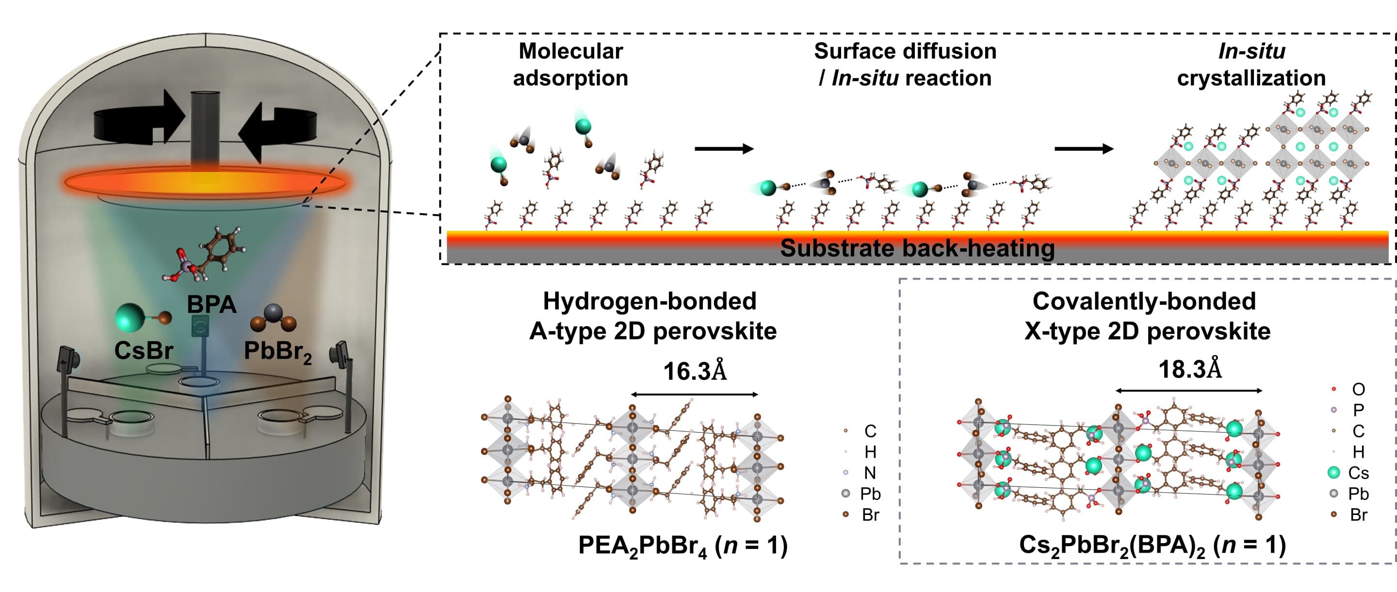
Image: TechXplore
A joint team from Seoul National University and the University of Cambridge says it has built a vapor-deposited perovskite LED with world-leading efficiency, tackling one of the biggest obstacles to bringing perovskites into mainstream display manufacturing.
According to Seoul National University College of Engineering, the team was led by Professor Tae-Woo Lee of SNU’s Department of Materials Science and Engineering and Professor Samuel D. Stranks of the University of Cambridge. Their results were published July 1 in Nature Nanotechnology.
Perovskites have long been seen as promising display materials because they combine high efficiency, vivid color emission and compatibility with manufacturing methods already used for OLEDs. The sticking point has been vacuum deposition: during that process, perovskite crystals can grow too quickly and unevenly, producing mixed phases, lower efficiency and weaker color purity.
How the X-type emitter works
To address that, the researchers designed a new X-type quasi-two-dimensional perovskite emitter. They introduced X-type spacer organic molecules that coordinate strongly with central lead ions during crystallization, helping suppress disordered growth and favor the most energetically stable crystal phase.

Recommended reading
24 travel gadgets PCWorld says are worth packing
The team also built a hetero-scaffold by chemically bonding the X-type spacer molecules with lithium fluoride (LiF). The idea is to guide crystal growth more uniformly across the substrate and reduce random phase formation during deposition.
Performance and display manufacturing potential
Using that approach, the team reported perovskite films with a photoluminescence quantum yield exceeding 85%. The resulting devices reached:
- 21.9% external quantum efficiency (EQE)
- 16.8 nm emission linewidth
- high efficiency alongside high color purity
The researchers said this represents world-leading performance among vapor-deposited PeLEDs.
The team also said the devices can be fabricated on large-area substrates, flexible platforms and patterned structures, which matters because industrial display production demands uniform thin films, precise thickness control and compatibility with existing process lines.
Lee said the study establishes a new emitter design based on how perovskite precursors react and crystallize on a substrate during vacuum deposition.
“This study is significant because it provides a fundamental understanding of how perovskite precursors react and crystallize on a substrate during vacuum deposition and, based on this understanding, establishes a new X-type quasi-2D perovskite emitter design. By realizing perovskite light-emitting devices with world-leading efficiency and color purity through a vacuum-deposition process compatible with existing OLED manufacturing infrastructure, this work is expected to provide a key technological foundation for accelerating the practical implementation of ultra-high-resolution displays and AR/VR microdisplays.”
The paper is “Halide-site-substituting spacer creates quasi-two-dimensional perovskites for vapour-deposited light-emitting diodes” by Chan-Yul Park et al., published in Nature Nanotechnology (2026) with DOI 10.1038/s41565-026-02208-y.

Computing Editor
Tomas lives in the terminal. He covers chips, laptops, and operating systems with a focus on performance and efficiency. He reads kernel changelogs the way other people read fiction, and he's always on the hunt for the perfect mechanical keyboard switch. If it processes data, Tomas has an opinion on it.
via TechXplore