• 2 min read
Silicon photonics gets a cleaner path to mixed materials
Researchers say micro-transfer printing could ease a key silicon photonics bottleneck by adding non-silicon components without breaking CMOS manufacturing.
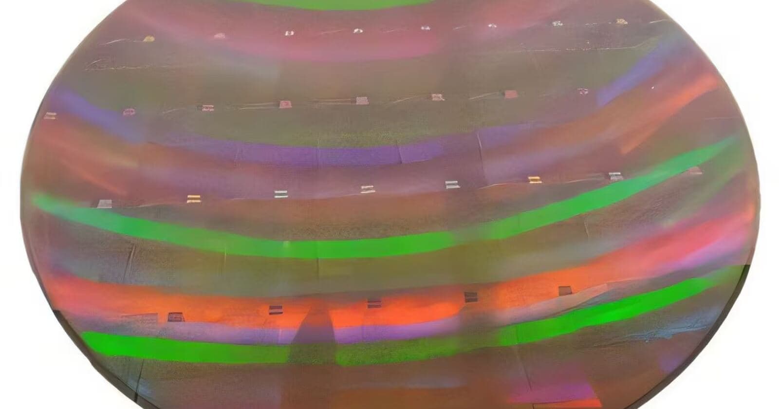
Image: ITzine
Researchers have outlined a way to tackle one of silicon photonics' biggest engineering problems: adding materials with very different properties to a silicon chip without disrupting the standard CMOS manufacturing flow.
The approach, described in the Journal of Lightwave Technology, uses micro-transfer printing (MTP). Instead of trying to build every optical function directly into silicon, manufacturers first fabricate thin-film devices separately, then move those tiny parts onto a silicon photonics platform to assemble a single chip from heterogeneous components.
That matters most in data centers and AI accelerators, where conventional electrical interconnects are increasingly constrained by speed and latency. Silicon is excellent for mass production, but by itself it cannot deliver every function needed in a complex photonic system. The industry has been trying to work around that for years through methods such as hybrid integration and chiplet-style assembly.
With MTP, the process works at micron scale. An elastomer stamp picks up miniature devices from a source wafer and places them onto a target silicon substrate. After transfer, the parts are fixed in place through adhesive or direct bonding. The result is a photonic system in which different materials handle different jobs while operating as one device.
That opens the door to combining components such as:

Recommended reading
Plastic additive boosts stretchable OLEDs to near 100% efficiency
- III-V semiconductor elements
- lithium niobate modulators
- other specialized photonic building blocks
The paper also points to practical use cases, including optical and microwave signal processing, gallium arsenide lasers for VR, quantum technologies, and microwave photonics, plus the integration of lithium niobate modulators with silicon nitride photonic circuits.
This is not just a lab demo. Silicon photonics is already used in photonic integrated circuits for telecommunications and data centers, and demand is being pushed higher by rising AI compute loads. The team also introduced a pilot line intended to refine the key MTP steps for mass production.
The harder part comes next: proving stable yield, reliability, fast assembly, and compatibility with existing industrial infrastructure. If those metrics hold up at production scale, chipmakers could build more complex silicon photonic systems without giving up the scalability of the CMOS ecosystem. In a market where moving data faster inside the data center matters more and more, that could be a bigger advantage than another paper increase in clock speed.

Computing Editor
Tomas lives in the terminal. He covers chips, laptops, and operating systems with a focus on performance and efficiency. He reads kernel changelogs the way other people read fiction, and he's always on the hunt for the perfect mechanical keyboard switch. If it processes data, Tomas has an opinion on it.
via ITzine