• 2 min read
TSMC’s 2nm line is 4x busier than 3nm was
TSMC says pre-launch demand for its 2nm N2 process is four times higher than 3nm at the same stage, driven by GAAFET gains.
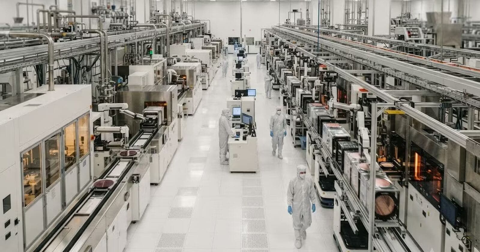
Image: ITzine
TSMC has already built a queue for its 2nm N2 process, with the number of prepared chip projects four times higher than the 3nm platform had at the same stage. That is a clear signal for the semiconductor industry: major customers are rushing to lock in capacity even before the node fully ramps in mass production.
Part of the demand comes from a bigger architectural shift. N2 will be TSMC’s first mass-market node to use GAAFET transistors, replacing FinFET. According to TSMC, the new process can deliver up to 15% higher performance at the same power, or cut power use by up to 30% at the same performance. The company also says transistor density will rise by about 15%.
In practical terms, that gives chip designers room to pack more logic into the same die, or keep chip sizes under control while adding more cores, cache, and accelerators. For customers such as Apple and AMD, that directly affects battery life, thermal limits, and manufacturing cost.
TSMC began mass production of N2 in the fourth quarter of 2025, but the new node is still making only a small contribution to revenue. The company’s 5nm and 3nm families remain the main business, contributing about 33% and 30% of quarterly revenue respectively.
Why demand is rising so quickly
TSMC is bringing 2nm to market as flagship chips run harder into limits around power and physics. Higher clocks are becoming more expensive, while performance gains increasingly come from larger die areas and heavier cooling. For smartphones, servers, and AI accelerators, that translates directly into battery life, rack density, and final device cost.
Recommended reading
PsiQuantum bets on light for a 100-cabinet quantum computer
That helps explain why large customers want early slots. Based on public information, AMD is preparing EPYC Venice server processors on N2, while Apple is expected to use the technology for the A20 Pro in the iPhone 18 Pro line. In both cases, even modest efficiency gains can turn into a meaningful advantage across an entire product generation.
The early surge matters for TSMC for another reason: competition at the leading edge is intensifying. Samsung is pushing its own 2nm GAA plans, and Intel is preparing 18A. At the same time, chip companies are increasingly splitting orders across multiple foundries to reduce dependence on a single supplier.
Against that backdrop, a fourfold increase in early projects looks like more than enthusiasm for one node. It also looks like a bid to secure capacity years in advance. TSMC has already mapped out the rest of the platform: N2P is due later in 2026, N2X is planned for 2027, and N2U is scheduled for 2028.

Computing Editor
Tomas lives in the terminal. He covers chips, laptops, and operating systems with a focus on performance and efficiency. He reads kernel changelogs the way other people read fiction, and he's always on the hunt for the perfect mechanical keyboard switch. If it processes data, Tomas has an opinion on it.
via ITzine